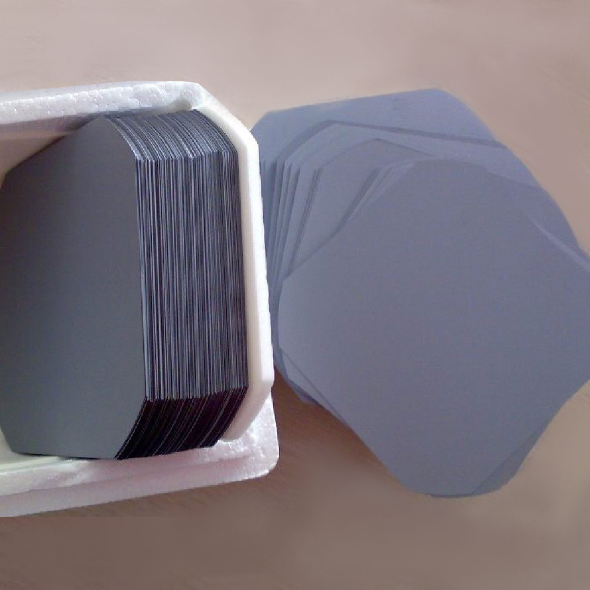

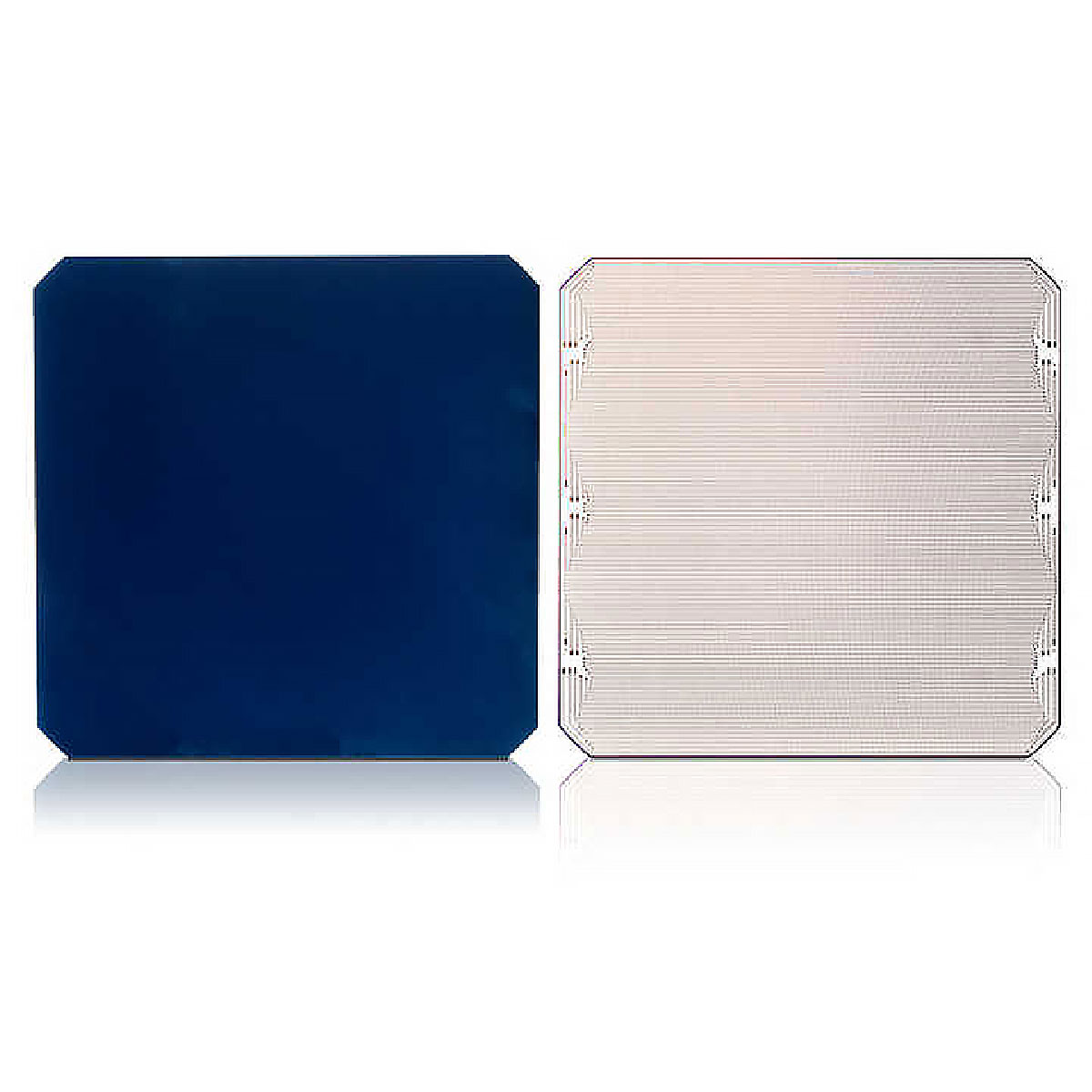
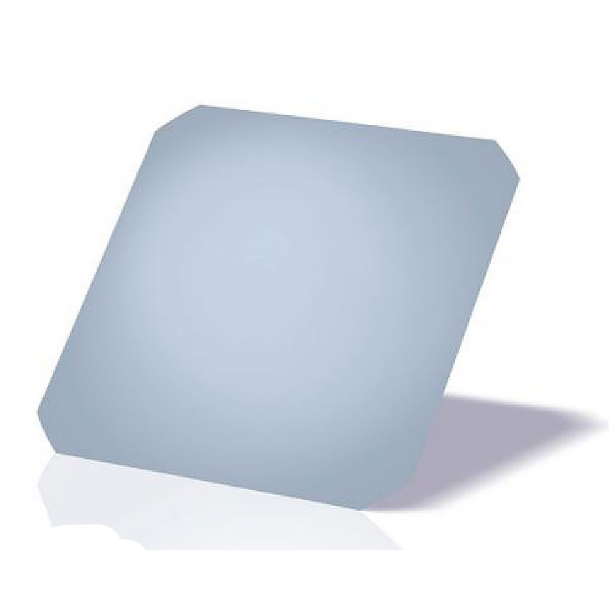


Description
|
|
General Specifications about Solar Wafer |
||||||
|
|
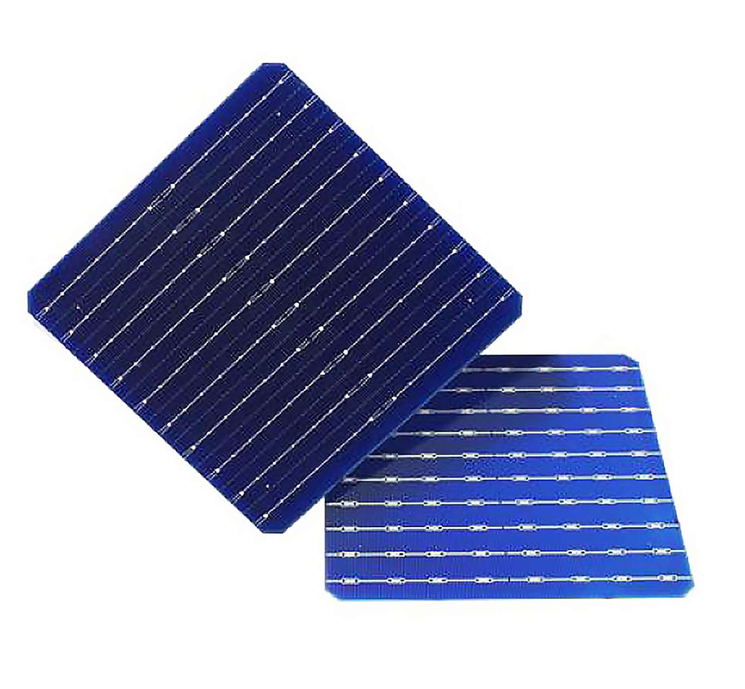
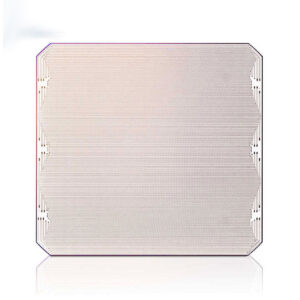
Types of Solar Wafers: |
||||||
|
|
– |
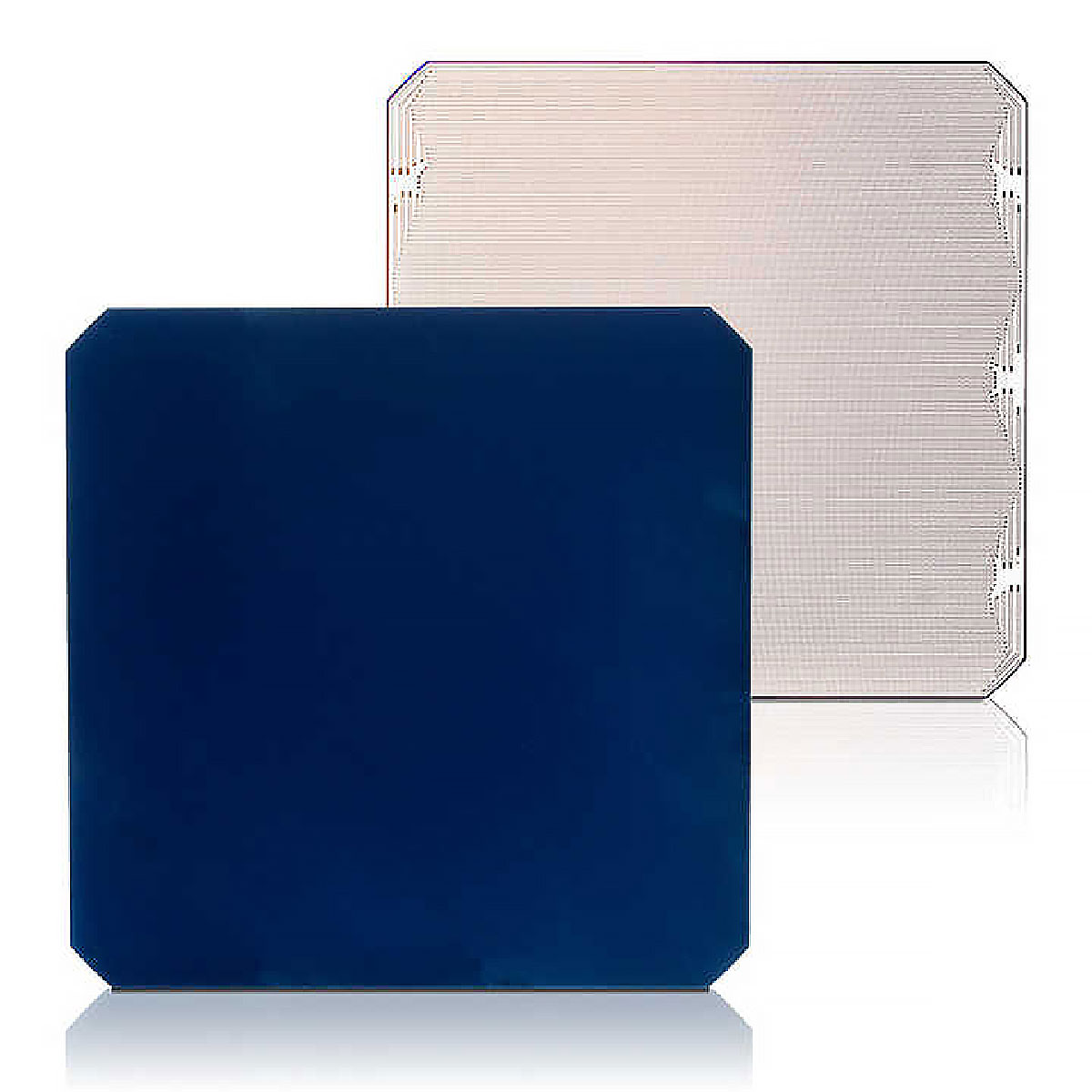
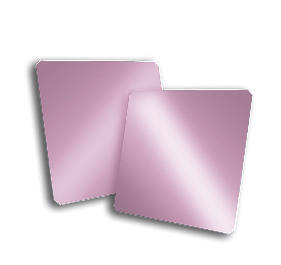
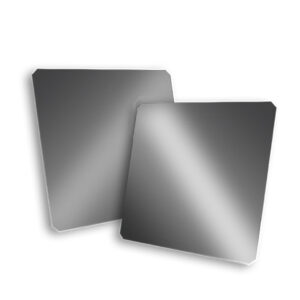
Monocrystalline: |
|||||
|
|
Cut from a single, continuous crystal of silicon, offering higher efficiency due to a uniform crystal structure. |
||||||
|
|
– |
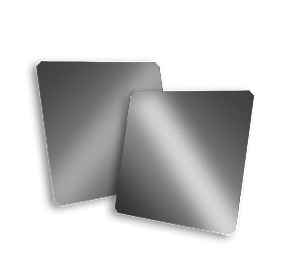
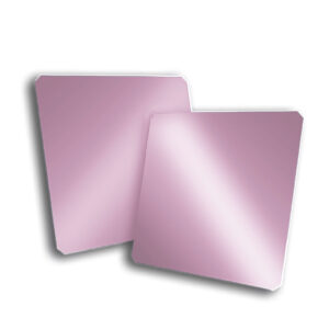
Polycrystalline: |
|||||
|
|
|
Made from multiple silicon crystals, generally less expensive but with slightly lower efficiency. |
|||||
|
|
Common Wafer Sizes: |
||||||
|
|
– |
156.75mm x 156.75mm (M2): |
|||||
|
|
– |
A widely used size, but some manufacturers are transitioning to larger formats. |
|||||
|
|
– |
158.75mm x 158.75mm (G1): |
|||||
|
|
– |
A popular size due to compatibility with existing module designs. |
|||||
|
|
– |
166mm x 166mm (M6): |
|||||
|
|
– |
A larger wafer size, gaining traction in the market. |
|||||
|
|
– |
182mm x 182mm (M10): |
|||||
|
|
– |
Another larger format, offering higher power output. |
|||||
|
|
– |
210mm x 210mm (G12): |
|||||
|
|
– |
A large format wafer designed for increased power generation and system efficiency. |
|||||
|
|
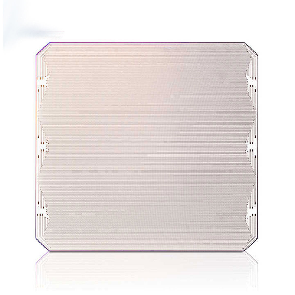
Key Specifications: |
||||||
|
|
– |
Material: Monocrystalline or Polycrystalline silicon. |
|||||
|
|
– |
Size: Can range from 156mm to 210mm (or larger). |
|||||
|
|
– |
Thickness: Typically, around 150-200 micrometers (µm). |
|||||
|
|
– |
Resistivity: Measured in ohm-centimeters (Ω·cm), typically between 0.4 and 2.0 Ω·cm. |
|||||
|
|
– |
Lifetime: Minority carrier lifetime, measured in microseconds (µs), affects cell efficiency. |
|||||
|
|
– |
Oxygen and Carbon Concentration: Impurity levels that can impact performance. |
|||||
|
|
– |
Orientation: Crystalline orientation, often <100> ±3°. |
|||||
|
|
– |
TTV (Total Thickness Variation): Measures thickness uniformity. |
|||||
|
|
– |
Saw Mark Depth: Indicates the quality of the cutting process. |
|||||
|
|
– |
Warp and Bow: Measures flatness, with lower values indicating better quality. |
|||||
|
|
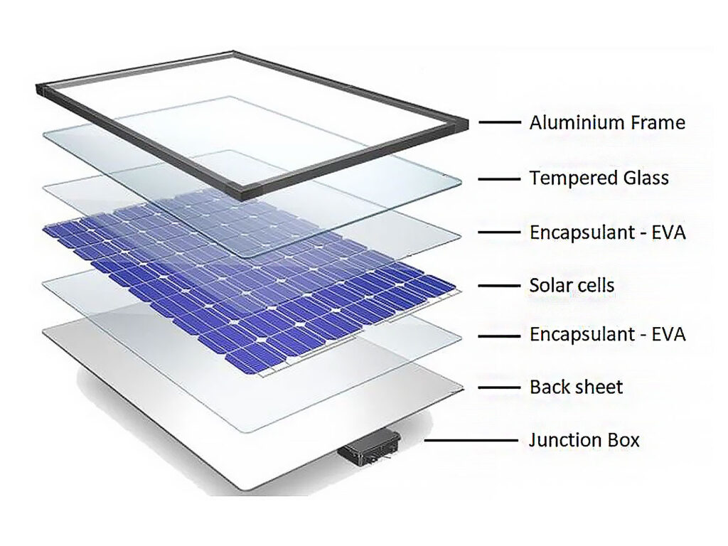
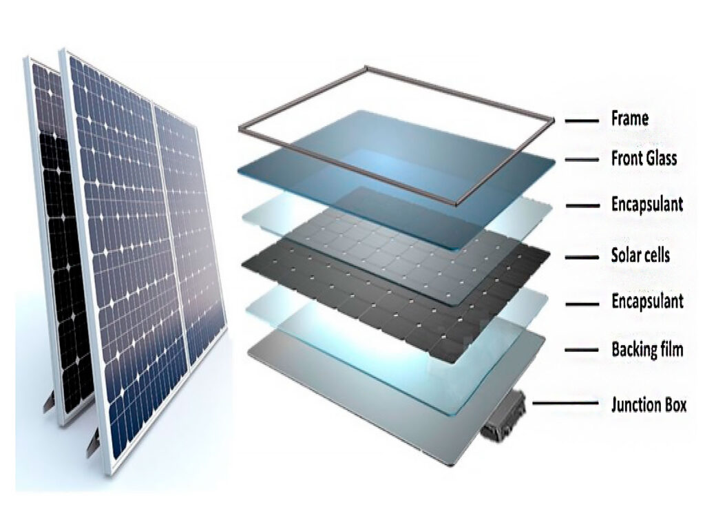
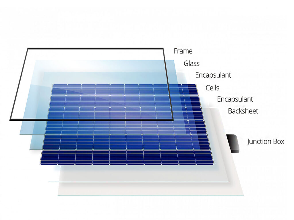
Wafer properties: |
||||||
|
|
– |
Made of pure silicon (either monocrystalline or polycrystalline). |
|||||
|
|
– |
Its thickness is typically between 120 and 200 micrometers. |
|||||
|
|
– |
It is electrically and optically processed to convert sunlight into electrical current. |
|||||
|
|
– |
Note: Wafer technologies have evolved in recent years to become thinner and more efficient, helping improve solar panel performance and reduce production costs |
|||||
|
|
These specifications may vary slightly depending on the manufacturer, customer requirements, and cell design (e.g., PERC, TOPCon, HJT). |
||||||
|
|
|
||||||
|
|
Typical Specification of Monocrystalline Silicon Solar Wafers |
||||||
|
|
Parameter |
Specification |
|||||
|
|
Material |
Monocrystalline Silicon |
|||||
|
|
Crystal Orientation |
⟨100⟩ or ⟨111⟩ |
|||||
|
|
Doping Type |
p-type (Boron) or n-type (Phosphorus) |
|||||
|
|
Resistivity |
0.5 – 3 Ω·cm (for p-type) or 1 – 10 Ω·cm (n-type) |
|||||
|
|
Wafer Size |
156.75 mm × 156.75 mm (6-inch standard) |
|||||
|
|
Wafer Thickness |
160 – 180 μm |
|||||
|
|
Surface Texture |
Pyramidal (acid or alkali etched) |
|||||
|
|
Edge |
Rounded corners (pseudo-square shape) |
|||||
|
|
TTV (Total Thickness Variation) |
< 20 μm |
|||||
|
|
Saw Damage |
Removed (via surface etching) |
|||||
|
|
Lifetime (Minority Carrier) |
> 1 μs (depends on quality grade) |
|||||
|
|
Oxygen Content |
< 1e18 atoms/cm³ |
|||||
|
|
Carbon Content |
< 5e17 atoms/cm³ |
|||||
|
|
Warp/Bow |
< 20 μm |
|||||
|
|
|
||||||
|
|
Examples of specifications for some types of Solar Wafers |
||||||
|
|
|
||||||
|
|
P Type 210 (Size: 210±0.25mm) |
||||||
|
|
|
||||||
|
|
|
||||||
|
|
KEY FEATURES |
||||||
|
|
– Mature process matched with advanced equipment |
||||||
|
|
– Customizable, fast delivery to meet customer needs |
||||||
|
|
– Low attenuation process |
||||||
|
|
Material properties |
||||||
|
|
Item(unit) |
Specification |
Inspection method |
||||
|
|
Conductivity Type |
P |
PN testing machine |
||||
|
|
Dopant |
Gallium |
/ |
||||
|
|
Crystallinity |
Monocrystalline |
Preferential etch techniques (ASTM F47-88) |
||||
|
|
Etch pit density (dislocation density) |
<500cm-2 |
Preferential etch techniques (ASTM F47-88) |
||||
|
|
Surface orientation |
<100>±3° |
X-ray diffraction method |
||||
|
|
Side orientation |
<010>, <001>±3° |
X-ray diffraction method |
||||
|
|
Oxygen contents (ppma) |
≤16 |
FTIR (ASTM F121-83) |
||||
|
|
Carbon contents (ppma) |
≤1 |
FTIR (ASTM F123-91) |
||||
|
|
Electrical properties |
||||||
|
|
Item(unit) |
Specification |
Inspection method |
||||
|
|
Lifetime (us) |
70 |
BCT-400 |
||||
|
|
Resistivity (Q. cm) |
0.4-1.1 |
Automatic sorting machine |
||||
|
|
Rule of geometry properties |
||||||
|
|
Item(unit) |
Specification |
Inspection method |
||||
|
|
Geometry |
Quasi square |
/ |
||||
|
|
Bevel edge shape |
Right Angle |
/ |
||||
|
|
Square length (mm) |
210±0.25mm |
Automatic sorting machine |
||||
|
|
Diagonal length (mm) |
295±0.25mm |
Automatic sorting machine |
||||
|
|
Chamfer length projection (mm) |
1.41±0.5mm |
Automatic sorting machine |
||||
|
|
Verticality |
90±0.150° |
Automatic sorting machine |
||||
|
|
Thickness(μm) |
155 + 10/ – 10 |
Automatic sorting machine |
||||
|
|
Appearance Quality |
||||||
|
|
Item(unit) |
Specification |
Inspection method |
||||
|
|
Surface quality |
No visual defects |
Automatic sorting machine |
||||
|
|
Chipping |
No visual defects, No bright line Depth<0.3mm, Length <0.5mm; Count < 2/pcs, no V-chip |
Automatic sorting machine |
||||
|
|
Saw mark (μm) |
≤15 |
Automatic sorting machine |
||||
|
|
Warpage(μm) |
≤40 |
Automatic sorting machine |
||||
|
|
TTV(μm) |
≤25 |
Automatic sorting machine |
||||
|
|
Micro cracks / Holes |
None |
Automatic sorting machine |
||||
|
|
Unfilled corner |
None |
Automatic sorting machine |
||||
|
|
|
||||||
|
|
N Type 210 (Size: 210±0.25mm) |
||||||
|
|
|
||||||
|
|
|
||||||
|
|
KEY FEATURES |
||||||
|
|
– Low Oxygen Large Heat Field Process |
||||||
|
|
– High-efficiency wafers that match customers’ differentiated needs |
||||||
|
|
– Adequate capacity reserves |
||||||
|
|
Material properties |
||||||
|
|
Item(unit) |
Specification |
Inspection method |
||||
|
|
Conductivity Type |
N |
PN testing machine |
||||
|
|
Dopant |
Phosphorus |
/ |
||||
|
|
Crystallinity |
Monocrystalline |
Preferential etch techniques (ASTM F47-88) |
||||
|
|
Etch pit density (dislocation density) |
<500cm-2 |
Preferential etch techniques (ASTM F47-88) |
||||
|
|
Surface orientation |
<100>±3° |
X-ray diffraction method |
||||
|
|
Side orientation |
<010>, <001>±3° |
X-ray diffraction method |
||||
|
|
Oxygen contents (ppma) |
≤12 |
FTIR (ASTM F121-83) |
||||
|
|
Carbon contents (ppma) |
≤1 |
FTIR (ASTM F123-91) |
||||
|
|
Electrical properties |
||||||
|
|
Item(unit) |
Specification |
Inspection method |
||||
|
|
Lifetime (us) |
>800 |
BCT-400 |
||||
|
|
Resistivity (Q. cm) |
0.3-2.1 |
Automatic sorting machine |
||||
|
|
Rule of geometry properties |
||||||
|
|
Item(unit) |
Specification |
Inspection method |
||||
|
|
Geometry |
Quasi square |
/ |
||||
|
|
Bevel edge shape |
Right Angle |
/ |
||||
|
|
Square length (mm) |
210±0.25mm |
Automatic sorting machine |
||||
|
|
Diagonal length (mm) |
295±0.25mm |
Automatic sorting machine |
||||
|
|
Chamfer length projection (mm) |
1.41±0.5mm |
Automatic sorting machine |
||||
|
|
Verticality |
90±0.150° |
Automatic sorting machine |
||||
|
|
Thickness(μm) |
130 + 10/ – 10 |
Automatic sorting machine |
||||
|
|
Appearance Quality |
||||||
|
|
Item(unit) |
Specification |
Inspection method |
||||
|
|
Surface quality |
No visual defects |
Automatic sorting machine |
||||
|
|
Chipping |
No visual defects, No bright line Depth<0.3mm, Length <0.5mm; Count < 2/pcs, no V-chip |
Automatic sorting machine |
||||
|
|
Saw mark (μm) |
≤15 |
Automatic sorting machine |
||||
|
|
Warpage(μm) |
≤40 |
Automatic sorting machine |
||||
|
|
TTV(μm) |
≤25 |
Automatic sorting machine |
||||
|
|
Micro cracks / Holes |
None |
Automatic sorting machine |
||||
|
|
Unfilled corner |
None |
Automatic sorting machine |
||||
|
|
|||||||
|
N Type 210 (Size: 182*183.75±0.25mm) |
|||||||
|
|
|||||||
|
|
|||||||
|
|
KEY FEATURES |
||||||
|
|
– Low Oxygen Large Heat Field Process |
||||||
|
|
– High-efficiency wafers that match customers’ differentiated needs |
||||||
|
|
– Adequate capacity reserves |
||||||
|
|
Material properties |
||||||
|
|
Item(unit) |
Specification |
Inspection method |
||||
|
|
Conductivity Type |
N |
PN testing machine |
||||
|
|
Dopant |
Phosphorus |
/ |
||||
|
|
Crystallinity |
Monocrystalline |
Preferential etch techniques (ASTM F47-88) |
||||
|
|
Etch pit density (dislocation density) |
<500cm-2 |
Preferential etch techniques (ASTM F47-88) |
||||
|
|
Surface orientation |
<100>±3° |
X-ray diffraction method |
||||
|
|
Side orientation |
<010>, <001>±3° |
X-ray diffraction method |
||||
|
|
Oxygen contents (ppma) |
≤12 |
FTIR (ASTM F121-83) |
||||
|
|
Carbon contents (ppma) |
≤1 |
FTIR (ASTM F123-91) |
||||
|
|
Electrical properties |
||||||
|
|
Item(unit) |
Specification |
Inspection method |
||||
|
|
Lifetime (us) |
>800 |
BCT-400 |
||||
|
|
Resistivity (Q. cm) |
0.3-2.1 |
Automatic sorting machine |
||||
|
|
Rule of geometry properties |
||||||
|
|
Item(unit) |
Specification |
Inspection method |
||||
|
|
Geometry |
Quasi square |
/ |
||||
|
|
Bevel edge shape |
Right Angle |
/ |
||||
|
|
Square length (mm) |
182 / 183.75±0.25mm |
Automatic sorting machine |
||||
|
|
Diagonal length (mm) |
247±0.25mm |
Automatic sorting machine |
||||
|
|
Chamfer length projection (mm) |
7.51±0.5mm |
Automatic sorting machine |
||||
|
|
Verticality |
90±0.15° |
Automatic sorting machine |
||||
|
|
Thickness(μm) |
130 + 10/ – 10 |
Automatic sorting machine |
||||
|
|
Appearance Quality |
||||||
|
|
Item(unit) |
Specification |
Inspection method |
||||
|
|
Surface quality |
No visual defects |
Automatic sorting machine |
||||
|
|
Chipping |
No visual defects, No bright line Depth<0.3mm, Length <0.5mm; Count < 2/pcs, no V-chip |
Automatic sorting machine |
||||
|
|
Saw mark (μm) |
≤15 |
Automatic sorting machine |
||||
|
|
Warpage(μm) |
≤40 |
Automatic sorting machine |
||||
|
|
TTV(μm) |
≤25 |
Automatic sorting machine |
||||
|
|
Micro cracks / Holes |
None |
Automatic sorting machine |
||||
|
|
Unfilled corner |
None |
Automatic sorting machine |
||||
|
|
|
||||||
|
|
Comparison Between |
||||||
|
|
Feature |
Monocrystalline Silicon |
Polycrystalline Silicon |
||||
|
|
Crystal Structure |
Single, continuous crystal structure |
Multiple silicon crystals fused together |
||||
|
|
Color |
Dark black or deep blue with rounded edges |
Light to medium blue with square edges |
||||
|
|
Efficiency |
Higher (typically 18–23%) |
Lower (typically 15–18%) |
||||
|
|
Performance in Low Light |
Better |
Moderate |
||||
|
|
Temperature Tolerance |
Better performance at high temperatures |
Slightly more affected by heat |
||||
|
|
Material Waste in Production |
More waste due to precise cutting of cylindrical ingots |
Less waste, simpler cutting from blocks |
||||
|
|
Lifespan |
25+ years (same as poly, but retains performance better) |
25+ years |
||||
|
|
Cost |
Higher |
Lower |
||||
|
|
Space Efficiency |
More power per square meter (ideal for limited roof space) |
Less efficient use of space |
||||
|
|
Common Applications |
Residential rooftops, commercial systems, space-constrained areas |
Utility-scale, cost-sensitive projects |
||||